
Views: 0 Author: Site Editor Publish Time: 2026-08-03 Origin: Site


High-throughput continuous manufacturing faces a constant daily struggle. You must constantly balance production line speed against required image quality. Pushing belts faster traditionally increases costly false reject rates. Standard optics paired over line scan sensors often introduce severe edge distortion. They lack the sharp physical contrast needed to resolve micro-defects at the pixel level. This poor optical input renders high-end machine learning and software algorithms completely ineffective. Precision optics actually act as the foundational bottleneck for automated inspection systems. Upgrading your setup ensures maximum contrast. It eliminates peripheral distortion across the entire field. This upgrade provides machine vision software the raw, pristine data required for high-accuracy, high-speed decision-making. You will learn how precise lenses correct physical optical aberrations. We also cover strict mechanical integration constraints and practical steps to evaluate your next lens upgrade.
Managers constantly fight the yield-speed paradox on the factory floor. When you increase production line speed, image resolution typically drops. This operational reality frustrates plant engineers globally. You process materials faster, but defect escapes inevitably rise. Alternatively, automated systems might trigger excessive false rejects. Both scenarios harm overall line productivity.
Standard commodity lenses routinely fail under these extreme operating conditions. They cannot keep up when engineers pair them over modern 8K or 16K line scan cameras. These basic lenses simply cannot resolve sub-pixel details accurately. Furthermore, light often falls off significantly at the sensor edges. This darkening effect creates massive blind spots in your inspection zone.
When standard optics fail, shadows look like stains. Slight variations in material thickness appear as catastrophic tears. The vision system flags perfectly acceptable products. These false positives force production lines to halt unnecessarily. Human operators must then manually verify the rejected items. This manual review destroys the efficiency gains of automated manufacturing. The core issue almost always points back to poor optical resolution.
Many facilities try fixing detection issues through software algorithms. However, software is only as good as the optical input it receives. Artificial intelligence models cannot fix permanently blurred images. Deep learning defect detection networks cannot compensate for optically distorted source data. You must feed them clean, high-contrast data first. Investing in a High Resolution Line Scan Lens ensures your software receives highly reliable input. This hardware foundation empowers your sophisticated algorithms. They can finally perform at their absolute theoretical limits. You stop throwing away good products and stop shipping defective ones.
You must understand how physical optics manipulate incoming light. Modulation Transfer Function (MTF) determines actual visual contrast capabilities. High-resolution lenses maximize this critical MTF value across the entire sensor surface. They maintain sharp contrast between closely spaced microscopic lines. This capability represents the ultimate metric for distinguishing a true defect from background noise. If your MTF drops, defects blend seamlessly into the background material. You lose the physical ability to spot scratches, dents, or discolorations.
You also need perfect edge-to-edge optical sharpness. Standard lenses lose sharp focus near the outer perimeter. Specialized optical designs prevent this frustrating vignetting effect. They stop image degradation at the sensor's extreme extremities. This uniformity ensures highly accurate detection across very wide materials. You can inspect wide webs of textiles, metallic foils, and float glass perfectly. Every single pixel receives equal light and crisp focus.
Precision glass plays another strictly vital role in automated inspection. It corrects both chromatic and spherical optical aberrations. These advanced lenses align different color wavelengths precisely. They focus scattered light rays onto exact planar points. This correction is completely non-negotiable when you inspect color-sensitive defects. For example, sorting subtle color shifts in printed packaging requires perfect wavelength alignment. It is equally critical for examining highly reflective surfaces. Standard lenses scatter this intense light, causing a glowing optical haze. Precision optics cut right through the glare to reveal underlying defects.
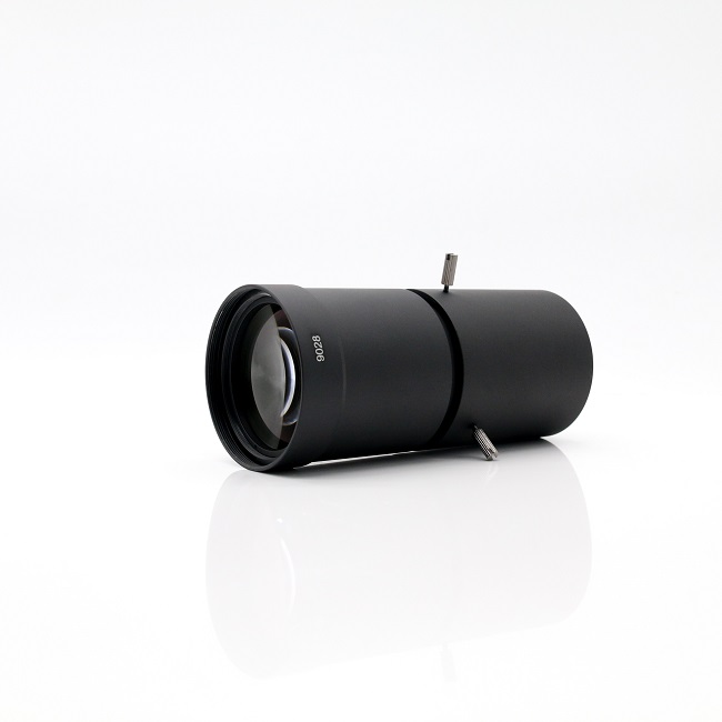
The automated optical inspection (AOI) environment demands extreme precision today. High-density interconnect (HDI) printed circuit boards pack components incredibly tight. This dense micro-architecture leaves absolutely zero margin for visual errors. Standard machine vision systems often overlook microscopic faults in these modern layouts. The copper traces are simply too narrow for basic lenses.
A dedicated PCB AOI Inspection Lens specifically targets these demanding physical requirements. It easily captures dangerous micro-cracks in the board substrate. It spots tiny bridging issues between adjacent copper pins. It also identifies microscopic solder joint irregularities perfectly. Standard lenses routinely miss these exact details because they lack resolving power.
You must also overcome severe surface reflectivity constraints during inspection. Copper traces and solder joints create complex, harsh specular reflections. These harsh reflections often blind standard industrial cameras entirely. High-resolution optics manage this intense glare highly efficiently. They feature advanced anti-reflective glass coatings. These coatings handle uneven light distribution without losing critical defect contrast. You see the physical fault clearly despite the bright metallic background. This capability dramatically reduces false positive rates on the busy factory floor. Engineers spend far less time reviewing phantom board defects.
Upgrading your optics introduces specific physical engineering constraints. First, consider the strict illumination prerequisite. High-resolution optics demand significantly brighter light sources. You need highly uniform, intense LED line lights. This light intensity helps you maintain extremely short exposure times. Fast continuous web speeds mandate these short exposures to freeze target motion. If you upgrade the lens but keep weak lighting, moving images will blur immediately.
Next, you must prioritize sensor and pixel pitch matching. Engineers must match the lens resolving power to the specific camera sensor. We measure this resolving power precisely in line pairs per millimeter (lp/mm). You must align it exactly to the physical pixel size, such as 3.5µm or 5µm. Failing to match these exact specifications creates an immediate optical bottleneck. A phenomenal camera does absolutely nothing behind a weak lens.
You must also carefully manage the strict depth of field (DOF). High-resolution lenses typically operate with narrower depth of field margins. Material flutter becomes a significant problem on fast-moving webs. If your inspection material bounces up and down, it might exit the tight focal plane. You need precise tension control on roll-to-roll machines. Maintaining a perfectly flat inspection surface keeps the target completely inside the optical focal depth.
Finally, consider physical mechanical stability very carefully. High-magnification systems remain highly vulnerable to microscopic vibrations. Heavy machinery vibrates constantly in typical industrial production facilities. You absolutely need robust, industrial-grade mounting solutions. Loose mounts ruin optical alignment instantly. Even a fraction of a millimeter shift destroys your sharp focus. You should utilize secure Invar or heavy-duty mounting brackets designed for harsh environments.
Move beyond basic baseline specifications when selecting new optical equipment. You should evaluate lenses based on continuous yield improvement metrics. A successful optical upgrade dramatically reduces manual QA engineering reviews. Focus on actual performance returns rather than just looking at basic datasheet numbers. Better optics consistently mean fewer returned material batches.
Consider these key evaluation dimensions carefully during your selection process:
You should follow a tightly structured evaluation process. Here is a proven numbered list of steps for your proof-of-concept phase:
Optical Evaluation Metrics Summary
| Evaluation Metric | Optimal Target Standard | Impact on Detection Accuracy |
|---|---|---|
| Optical Distortion | < 0.1% across field | Prevents physical warping at image edges. Ensures highly accurate spatial measurement. |
| Resolving Power (lp/mm) | Matches Sensor Pixel Pitch | Ensures the lens delivers enough optical detail to saturate individual sensor pixels. |
| Vignetting Control | > 80% Edge Illumination | Maintains uniform image brightness. Reduces annoying false positives near web edges. |
| Chromatic Aberration | Fully Apochromatic Design | Keeps color channels perfectly aligned. Crucial for identifying subtle discoloration defects. |
Defect detection accuracy always starts precisely at the photon level. Your high-end camera sensors are completely wasted on sub-par lenses. If the glass cannot resolve the physical defect, the software cannot analyze it. Optical clarity acts as the ultimate physical ceiling for your entire inspection system.
Remember this final critical decision consideration. A high-resolution line scan lens is not a standalone magical fix. However, it serves as the critical enabler of a fully optimized machine vision system. It bridges the crucial gap between raw physical material and intelligent software analysis.
We strongly encourage engineers to consult with dedicated optical specialists early. You should model your specific physical working distance carefully. Map out your exact sensor size and mechanical constraints. Define your absolute minimum defect resolution requirements well before finalizing any procurement. Taking these proactive steps guarantees a robust, highly accurate inspection pipeline.
A: You must match the lens’s maximum image circle (sensor size coverage) and its resolving power (in line pairs per millimeter) to the specific pixel pitch of your sensor to prevent vignetting and optical bottlenecking.
A: Area scan lenses are optimized for a rectangular format. Line scan sensors are typically much longer (up to 80mm+); using an area scan lens will result in severe light fall-off, distortion, and blurring at the edges of the line array.
A: Yes, provided your lighting can be scaled. A high-resolution lens captures sharper contrast, allowing inspection software to make accurate defect decisions faster, which facilitates higher continuous web speeds without sacrificing yield.


